SK Hynix Unveils First HBF Standard Specifications With Sandisk, Presenting AI Memory Solutions At ‘FMS 2026’

Tenth-generation (V10) 375-layer 4D NAND unveiled for the first time at exhibition booth, offering a 2.5 times increase in power efficiency
By Cyber Era NG Special Correspondents
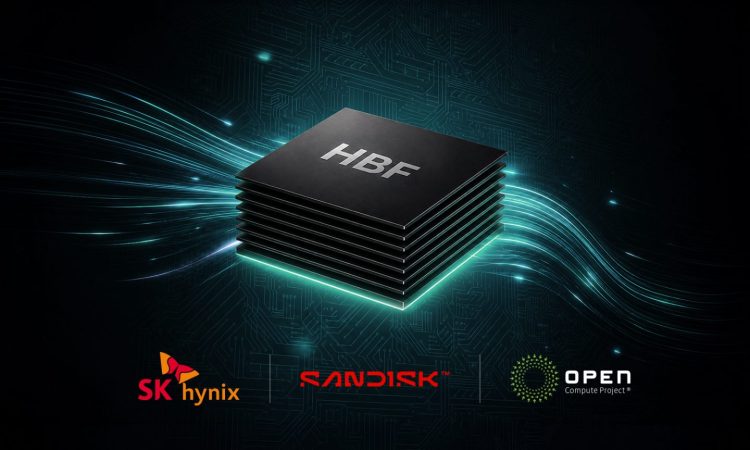
SK hynix Inc. has announced in collaboration with Sandisk that it has unveiled the first standard specifications for High Bandwidth Flash (HBF), a next-generation storage technology.
The announcement coincides with the opening of ‘FMS (Future of Memory and Storage) 2026,’ held at the Santa Clara Convention Center in California from August 4 to 6 (local time). The company is set to present HBF as a key technology to overcome memory bottlenecks in the AI era through keynote speeches and panel discussions during the event.
HBF technology is a new memory layer between HBM and SSDs. It enables high-speed data transfer similar to HBM while significantly expanding capacity by leveraging NAND technology. With the expansion of AI inference driving a surge in data volumes to process, HBF is gaining attention as a technology that simultaneously resolves bandwidth and capacity scalability challenges.
This milestone comes about six months after launching the consortium in February this year, following the initial standardization partnership with Sandisk in August 2025. Capacity specifications cover up to 512GB based on two stack configurations (8-high and 16-high NAND dies). Bandwidth is categorized into three grades (Grade1~3), delivering scalable performance from approximately 0.4TB/s to 3.0TB/s.
A key highlight is the interconnect linking HBF technology and processors. HBF technology adopts UCIe, an industry standard connection interface, laying the groundwork to flexibly integrate HBF technology across different processor types, including GPUs and CPUs.
* UCIe (Universal Chiplet Interconnect Express): An open standard interface specification designed for high-speed interconnection of heterogeneous semiconductor chiplets.
The standard also outlines
▲connection interfaces and electrical characteristics,
▲reliability and packaging guidelines for HBF die stack process,
▲software I/O guidelines.
The specification was disclosed through the Open Compute Project (OCP), world’s largest open data center technology initiative, positioning it as an open standard for the entire industry rather than a proprietary technology.
SK hynix plans to leverage this release to expand the adoption of HBF technology in the AI storage market and foster the surrounding ecosystem. With Google and Tenstorrent currently participating in the HBF consortium, the consortium aims to expand its reach while enhancing technical maturity and market acceptance based on open collaboration.
“With the rapid spread of AI applications, we are at a point where overall data processing structures must be redesigned,” said SK hynix Executive Vice President and Head of Solution Development Kim Chun-sung, adding, “Through HBF, SK hynix will expand the boundaries between memory and storage and contribute to building new architectures that enhance overall system efficiency.”